- One Of The Major Applications Of P N Diodes Discussed In Class Is Rectification Conversion Of Ac To Dc A Large Signal 1 (93.56 KiB) Viewed 31 times
- One Of The Major Applications Of P N Diodes Discussed In Class Is Rectification Conversion Of Ac To Dc A Large Signal 2 (44.1 KiB) Viewed 31 times
- One Of The Major Applications Of P N Diodes Discussed In Class Is Rectification Conversion Of Ac To Dc A Large Signal 3 (12.86 KiB) Viewed 31 times
One of the major applications of p-n diodes discussed in class is rectification - conversion of AC to DC. A large signal diode - with a large p-n junction (depletion) region- that allows for increased forward current carrying capacity (forward resistance of a few Ohms) and reverse blocking resistance of few Mega Ohms is needed. Such diodes are useful for low frequency applications such as rectifiers, inverters, battery charging devices, etc. For typical ratings of a diode visit this link:
https://www.allaboutcircuits.com/textbo ... e-ratings/ Consider the following scenario. You are a solid state device expert working for ACME International Microelectronics Establishment (AIME). A customer approaches you to seek your advice on a low cost circuit that provides for a reasonable' rectification of an AC signal. From your experience, you know that she probably needs a half wave rectifier (low cost) that operates under the following conflicting criteria: (i) a diode with capacitance in a given range, (ii) a low forward resistance to keep power consumption by the diode to a minimum, (ii) an output voltage less than the peak input value. (iv) a reverse bias not exceeding the breakdown voltage and (v) an 50 Hz-60 Hz input frequency. You are expected to investigate a potential diode that meets these requirements. Your task is to explore the optimum characteristics of such a diode. Submit a brief report on your approach to addressing this task. What you plan to do, how you would interpret the customer's need and how you would proceed to find at least one choice of a diode that meets her requirements. To facilitate analysis, consider the following steps: 1. List the general characteristics of p-n junction diodes - forward current, forward voltage, reverse resistance, capacitance, temperature stability, among others. 2. Investigate the literature to explore at least three different diodes that, when a diode is made out of it, provides the optimum range of capacitance values. 3. Compute the relevant quantities for these diodes that meet the customer's requirements. 4. Write a concise but detailed report of your findings along with a summary and a rationale for your choice(s)/recommendations. The attached rubric will be employed to assess your submission. Your report should be properly formatted, and should include, at a minimum: Title Page. Abstract, Introduction and Motivation, Proposed Approach to the Assigned Project, Relevant Equations and Computations, Analysis of Results, Conclusions and References/Bibliography. Identify specific learning strategies employed in your deliberations. Included after the Rubric is a learning Styles Survey.
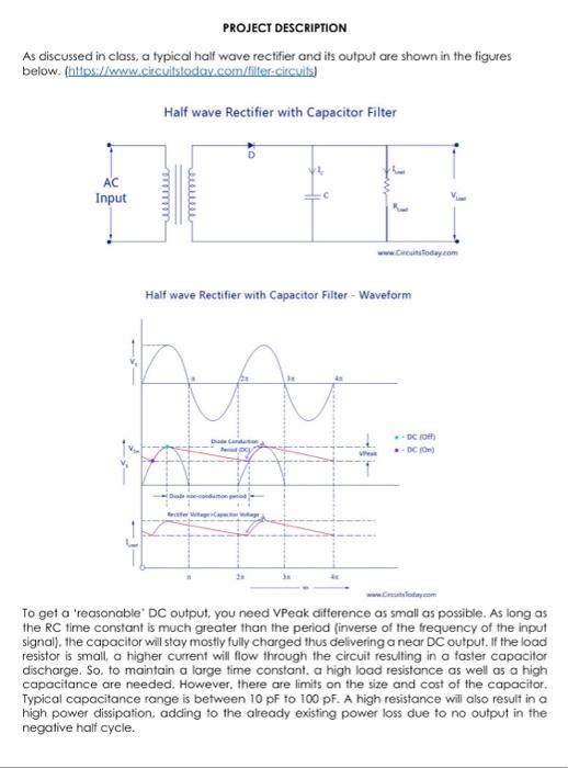
PROJECT DESCRIPTION As discussed in class, a typical half wave rectifier and its output are shown in the figures below. (
https://www.circuitstoday.com/filter-circuits) Half wave Rectifier with Capacitor Filter AC Input Half wave Rectifier with Capacitor Filter-Waveform -DC (off) Die Canton DI ĐỘNG Week Di To get a 'reasonable DC output, you need VPeak difference as small as possible. As long as the RC time constant is much greater than the period (inverse of the frequency of the input signal), the capacitor will stay mostly fully charged thus delivering a near DC output. If the load resistor is small, a higher current will flow through the circuit resulting in a faster capacitor discharge. So, to maintain a large time constant, a high load resistance as well as a high capacitance are needed. However, there are limits on the size and cost of the capacitor. Typical capacitance range is between 10 pF to 100 pF. A high resistance will also result in a high power dissipation, adding to the already existing power loss due to no output in the negative half cycle. [ J
www.Circuitstoday.com
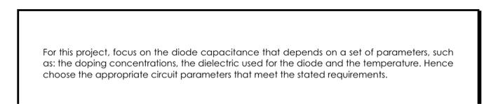
For this project, focus on the diode capacitance that depends on a set of parameters, such as: the doping concentrations, the dielectric used for the diode and the temperature. Hence choose the appropriate circuit parameters that meet the stated requirements.