Page 1 of 1
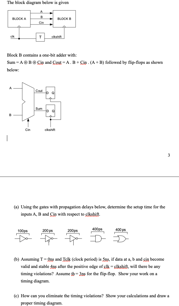
The block diagram below is given А B BLOCK A BLOCKB Cin clk T clkshift Block B contains a one-bit adder with: Sum = A B
Posted: Fri Apr 29, 2022 10:42 am
by answerhappygod
- 1 (65.99 KiB) Viewed 19 times
The block diagram below is given А B BLOCK A BLOCKB Cin clk T clkshift Block B contains a one-bit adder with: Sum = A B Cin and Cout=A. B+ Cin. (A + B) followed by flip-flops as shown below: А. Cout -Do Sum DO B Cin clkshift 3 (a) Using the gates with propagation delays below, determine the setup time for the inputs A, B and Cin with respect to clkshift. 100ps 200 ps 200ps 400ps 400 ps (b) Assuming T = Ons and Tclk (clock period) is 5ns, if data at a, b and cin become valid and stable 4ns after the positive edge of clk = clkshift, will there be any timing violations? Assume th=3ns for the flip-flop. Show your work on a timing diagram (c) How can you eliminate the timing violations? Show your calculations and draw a proper timing diagram