Page 1 of 1
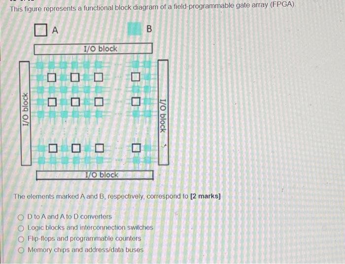
This figure represents a functional block diagram of a field-programmable gate array (FPGA). DA B I/O block 1/0 block I/
Posted: Fri Apr 29, 2022 8:52 am
by answerhappygod
- This Figure Represents A Functional Block Diagram Of A Field Programmable Gate Array Fpga Da B I O Block 1 0 Block I 1 (57.98 KiB) Viewed 46 times
This figure represents a functional block diagram of a field-programmable gate array (FPGA). DA B I/O block 1/0 block I/O block ロロロ 1/0 block The elements marked A and B, respectively, correspond to [2 marks] OD to A and A to D converters Logic blocks and interconnection switches Flip-flops and programmable counters O Memory chips and address/data buses