Page 1 of 1
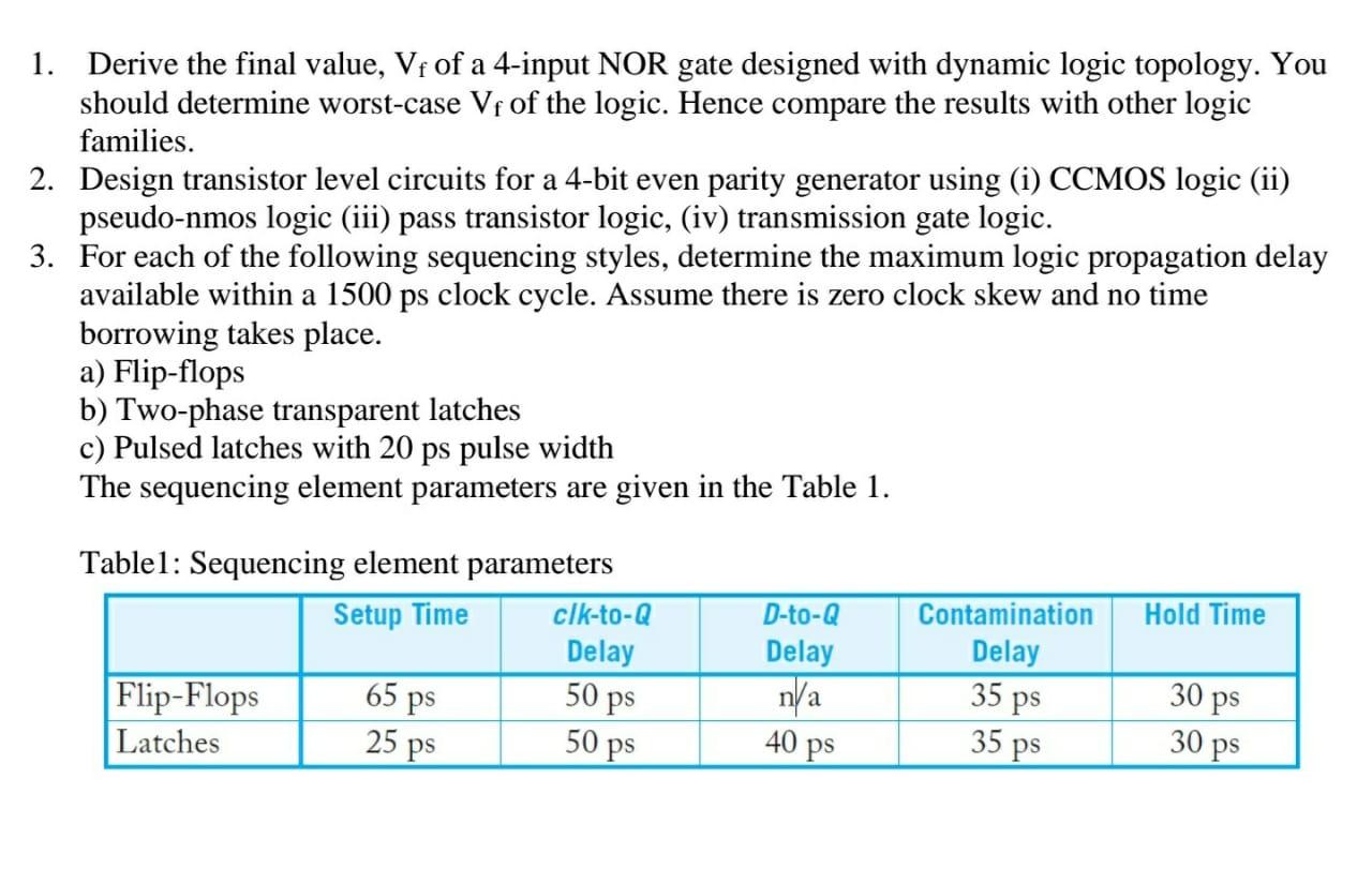
1. Derive the final value, Vf of a 4-input NOR gate designed with dynamic logic topology. You should determine worst-cas
Posted: Tue Apr 26, 2022 2:02 pm
by answerhappygod
- 1 Derive The Final Value Vf Of A 4 Input Nor Gate Designed With Dynamic Logic Topology You Should Determine Worst Cas 1 (117.49 KiB) Viewed 76 times
1. Derive the final value, Vf of a 4-input NOR gate designed with dynamic logic topology. You should determine worst-case Vf of the logic. Hence compare the results with other logic families. 2. Design transistor level circuits for a 4-bit even parity generator using (i) CCMOS logic (ii) pseudo-nmos logic (iii) pass transistor logic, (iv) transmission gate logic. 3. For each of the following sequencing styles, determine the maximum logic propagation delay available within a 1500 ps clock cycle. Assume there is zero clock skew and no time borrowing takes place. a) Flip-flops b) Two-phase transparent latches c) Pulsed latches with 20 ps pulse width The sequencing element parameters are given in the Table 1. Hold Time Tablel: Sequencing element parameters Setup Time clk-to-Q Delay Flip-Flops Latches 25 ps D-to-Q Delay n/a 65 ps Contamination Delay 35 ps 35 ps 50 ps 50 ps 30 ps 40 ps 30 ps