Page 1 of 1
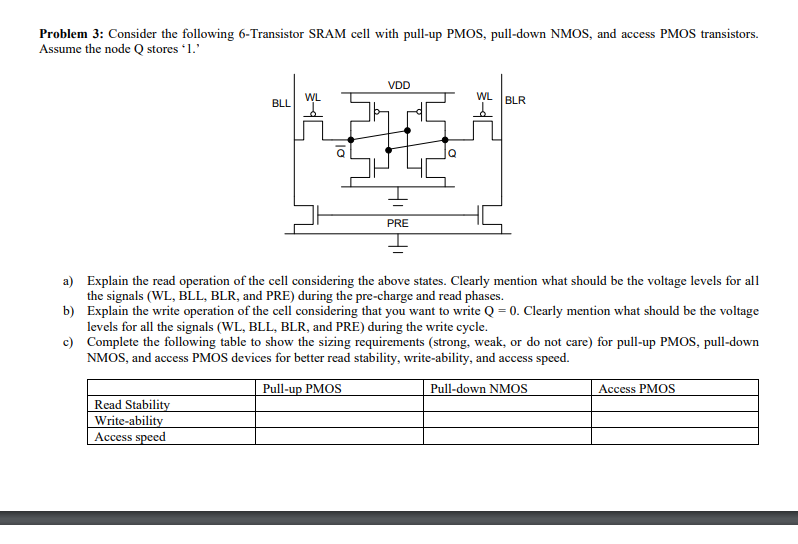
Problem 3: Consider the following 6-Transistor SRAM cell with pull-up PMOS, pull-down NMOS, and access PMOS transistors.
Posted: Tue Apr 26, 2022 2:00 pm
by answerhappygod
- Problem 3 Consider The Following 6 Transistor Sram Cell With Pull Up Pmos Pull Down Nmos And Access Pmos Transistors 1 (71.77 KiB) Viewed 38 times
Problem 3: Consider the following 6-Transistor SRAM cell with pull-up PMOS, pull-down NMOS, and access PMOS transistors. Assume the node Q stores 'l.' VDD BLL WL WL b BLR DI Q PRE 1 a) Explain the read operation of the cell considering the above states. Clearly mention what should be the voltage levels for all the signals (WL, BLL, BLR, and PRE) during the pre-charge and read phases. b) Explain the write operation of the cell considering that you want to write Q = 0. Clearly mention what should be the voltage levels for all the signals (WL, BLL, BLR, and PRE) during the write cycle. c) Complete the following table to show the sizing requirements (strong, weak, or do not care) for pull-up PMOS, pull-down NMOS, and access PMOS devices for better read stability, write-ability, and access speed. Pull-up PMOS Pull-down NMOS Access PMOS Read Stability Write-ability Access speed