Page 1 of 1
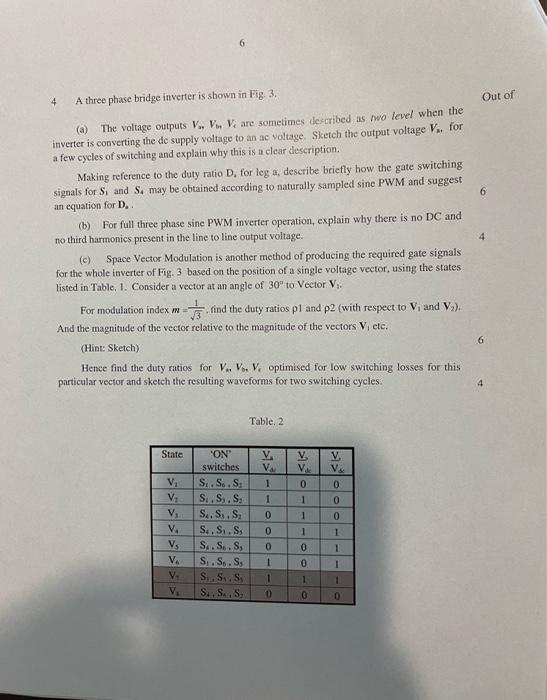
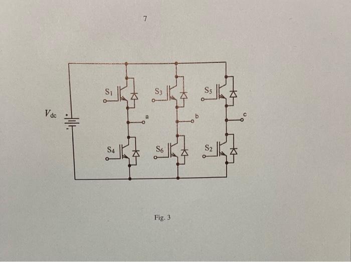
A three phase bridge inverter is shown in Fig. 3. (a) The voltage outputs V., V. V. are sometimes described as two level
Posted: Fri Jul 08, 2022 6:22 am
by answerhappygod
- A Three Phase Bridge Inverter Is Shown In Fig 3 A The Voltage Outputs V V V Are Sometimes Described As Two Level 1 (49.25 KiB) Viewed 44 times
- A Three Phase Bridge Inverter Is Shown In Fig 3 A The Voltage Outputs V V V Are Sometimes Described As Two Level 2 (30.42 KiB) Viewed 44 times
A three phase bridge inverter is shown in Fig. 3. (a) The voltage outputs V., V. V. are sometimes described as two level when the inverter is converting the de supply voltage to an ac voltage. Sketch the output voltage V.. for a few cycles of switching and explain why this is a clear description. 4 Making reference to the duty ratio D, for leg a, describe briefly how the gate switching signals for S₁ and Sa may be obtained according to naturally sampled sine PWM and suggest an equation for D.. (b) For full three phase sine PWM inverter operation, explain why there is no DC and no third harmonics present in the line to line output voltage. (c) Space Vector Modulation is another method of producing the required gate signals for the whole inverter of Fig. 3 based on the position of a single voltage vector, using the states listed in Table, 1. Consider a vector at an angle of 30" to Vector V₁. For modulation index m find the duty ratios p1 and p2 (with respect to V, and V₂). And the magnitude of the vector relative to the magnitude of the vectors V, etc. (Hint: Sketch) Hence find the duty ratios for V₁, V, V, optimised for low switching losses for this particular vector and sketch the resulting waveforms for two switching cycles. State V₁ V₁₂ V₁ V. V₁ V₁ V. V₁ 'ON' switches St. S.St S.S.S₂ Sa. Sy. S₂ Sa. S₁.Ss S.S.S, St. S. St S.S.S S. S. S Table. 2 V₂ Va 1 I 0 0 0 1 1 0 V Vac 0 1 1 1 -c 0 0 1 0 V IOOOKK V& 1 I 1 0 Out of 6 4 6
Vdc d 7 S4 S ܕܬܘ ܐܫ ܐܢܘ S5 Fig. 3