Page 1 of 1
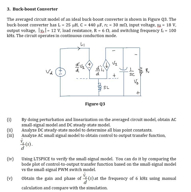
3. Buck-boost Converter The averaged circuit model of an ideal buck-boost converter is shown in Figure Q3. The buck-boos
Posted: Sun Jul 03, 2022 12:08 pm
by answerhappygod
- 3 Buck Boost Converter The Averaged Circuit Model Of An Ideal Buck Boost Converter Is Shown In Figure Q3 The Buck Boos 1 (83.68 KiB) Viewed 16 times
3. Buck-boost Converter The averaged circuit model of an ideal buck-boost converter is shown in Figure Q3. The buck-boost converter has L = 25 µH, C = 440 µF, rc = 30 m2, input voltage, va = 18 V, output voltage, |v|= 12 V, load resistance, R = 6 , and switching frequency fs: kHz. The circuit operates in continuous conduction mode. = 100 (i) (ii) (iii) (iv) (v) Vd (± 818 U₁ +1 212 чиет SL Figure Q3 √₂ + SC [50] ww + R By doing perturbation and linearization on the averaged circuit model, obtain AC small-signal model and DC steady-state model. Analyze DC steady-state model to determine all bias point constants. Analyze AC small signal model to obtain control to output transfer function, le(s). Using LTSPICE to verify the small-signal model. You can do it by comparing the bode plot of control-to-output transfer function based on the small-signal model vs the small-signal PWM switch model. Obtain the gain and phase of(s) at the frequency of 6 kHz using manual (s) a d calculation and compare with the simulation.