
- Ltm4657 Pin Functions Package Row And Column Labeling May Vary Among Module Products Review Each Package Layout Careful 1 (120.61 KiB) Viewed 47 times
- Ltm4657 Pin Functions Package Row And Column Labeling May Vary Among Module Products Review Each Package Layout Careful 2 (74.99 KiB) Viewed 47 times
- Ltm4657 Pin Functions Package Row And Column Labeling May Vary Among Module Products Review Each Package Layout Careful 3 (58.32 KiB) Viewed 47 times
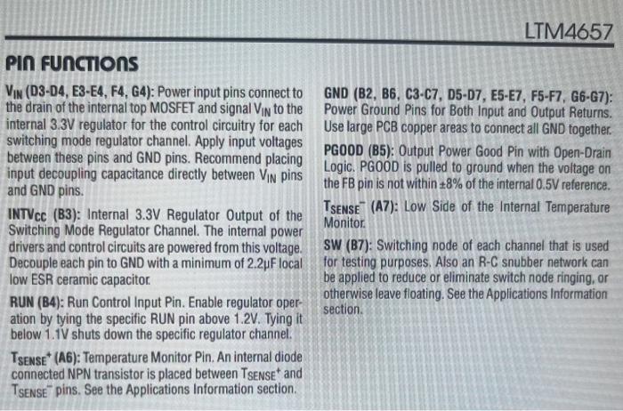
LTM4657 PIN FUNCTIONs PACKAGE ROW AND COLUMN LABELING MAY VARY AMONG Module PRODUCTS. REVIEW EACH PACKAGE LAYOUT CAREFULLY. VOUT (A1-A5, F3, G1-G3): Power Output Pins of the Switching Mode Regulator. Apply output load between these pins and GND pins. Recommend placing output decoupling capacitance directly between these pins and GND pins. See the Applications Information section for paralleling outputs. COMPb (F1): Internal Loop Compensation Network. Connect to COMPa to use the internal compensation in majority of applications. FREQ (E1): Switching Frequency Program Pin. Frequency is set internally to 500kHz. An external resistor can be placed from this pin to GND to increase frequency, or from this pin to INTVcc to reduce frequency. See the Applications Information section for frequency adjustment. COMPa (D1): Current control threshold and error ampli- fier compensation point of the switching mode regulator channel. The internal current comparator threshold is linearly proportional to this voltage. Tie the COMPa pins from different channels together for parallel operation. The device is internal compensated. Connect to COMPb to use the internal compensation. Or connect to a Type-ll C-R-C network to use customized compensation. FB (C1): The Negative Input of the Error Amplifier for the switching mode regulator This pin is internally con- nected to VOSNS with a 60.4k2 precision resistor. Output voltages can be programmed with an additional resistor between FB and VOSNS pins. In PolyPhase operation, tying the FB pins together allows for parallel operation. See the Applications Information section for details. VOSNS (B1): Positive Input to the Differential Remote Sense Amplifier. Internally, this pin is connected to FB with a 60.4k 0.5% precision resistor. See the Applications Information section for details. PHMODE (G5): Control Input to the Phase Selector of the Switching Mode Regulator Determines the phase rela- tionship between internal oscillator and CLKOUT. Tie it to INTVCC for 2-phase operation, tie it to GND for 3-phase operation, and tie it to INTVcc/2 for 4-phase operation. See Application Information section for details. TRACK/SS (E2): Output Tracking and Soft-Start Pin of the Switching Mode Regulator Allows the user to control the rise time of the output voltage. Putting a voltage below 0.5V on this pin bypasses the internal reference input to the error amplifier, instead it servos the FB pin to the TRACK voltage. Above 0.5V, the tracking function stops and the internal reference resumes control of the error amplifier. There's an internal 6uA pull-up current from INTVCC on this pin, so putting a capacitor here provides soft-start function. See the Applications Information sec- tion for details. MODE/CLKIN (D2): Discontinuous Mode Select Pin and External Synchronization Input to Phase Detector Tie MODE/CLKIN to GND for discontinuous mode of opera- tion. Floating MODE/CLKIN or tying it to a voltage above 1V will select forced continuous mode. Furthermore, con- necting MODE/CLKIN to an external clock will synchronize the system clock to the external clock and puts the part in forced continuous mode. See Applications Information section for details. VOSNS (C2): Negative Input to the Differential Remote Sense Amplifier. Connect an external resistor between FB and VOSNS pin to set the output voltage of the specific channel. See the Applications Information section for details. CLKOUT (F2): Output Clock Signal for PolyPhase Operation. The phase of CLKOUT with respect to CLKIN is determined by the state of the respective PHMODE pin. CLKOUT's peak-to-peak amplitude is INTV cc to GND. See Application Information section for details.
PIN FUNCTIOns VIN (D3-D4, E3-E4, F4, G4): Power input pins connect to the drain of the internal top MOSFET and signal VIN to the internal 3.3V regulator for the control circuitry for each switching mode regulator channel. Apply input voltages between these pins and GND pins. Recommend placing input decoupling capacitance directly between VIN pins and GND pins. INTVCC (B3): Internal 3.3V Regulator Output of the Switching Mode Regulator Channel. The internal power drivers and control circuits are powered from this voltage. Decouple each pin to GND with a minimum of 2.2μF local low ESR ceramic capacitor RUN (B4): Run Control Input Pin. Enable regulator oper- ation by tying the specific RUN pin above 1.2V. Tying it below 1.1V shuts down the specific regulator channel. TSENSE (A6): Temperature Monitor Pin. An internal diode connected NPN transistor is placed between TSENSE and TSENSE pins. See the Applications Information section. LTM4657 GND (B2, B6, C3-C7, D5-D7, E5-E7, F5-F7, G6-G7): Power Ground Pins for Both Input and Output Returns. Use large PCB copper areas to connect all GND together. PGOOD (B5): Output Power Good Pin with Open-Drain Logic. PGOOD is pulled to ground when the voltage on the FB pin is not within +8% of the internal 0.5V reference. TSENSE (A7): Low Side of the Internal Temperature Monitor. SW (B7): Switching node of each channel that is used for testing purposes. Also an R-C snubber network can be applied to reduce or eliminate switch node ringing, or otherwise leave floating. See the Applications Information section.
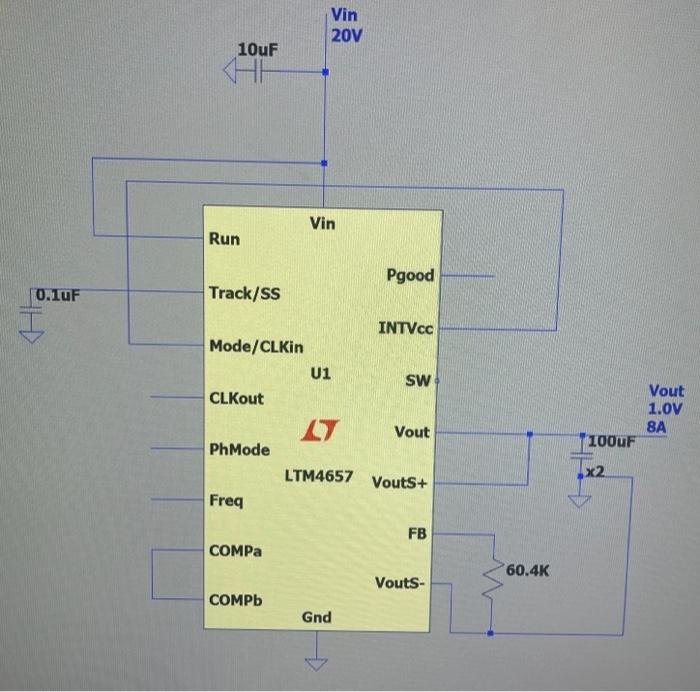
0.1uF 10uF Run Track/SS Mode/CLKin CLKout PhMode Freq COMPA COMPb Vin 20V Vin U1 Pgood Gnd INTVCC SW Vout LTM4657 Vouts+ FB Vouts- 60.4K 100uF Tx2 Vout 1.0V 8A