
- Use Pspice To Analyze The Half Wave Rectifier Circuit Shown Below Voff 0 Vamp 125 Freq 50 D Real Ci 250 Hf Www Ri 1050 1 (43.52 KiB) Viewed 37 times
Please answer both parts. Thank you.
- Use Pspice To Analyze The Half Wave Rectifier Circuit Shown Below Voff 0 Vamp 125 Freq 50 D Real Ci 250 Hf Www Ri 1050 2 (21.99 KiB) Viewed 37 times
Use PSpice to analyze the half-wave rectifier circuit shown below. VOFF-0 VAMP 125 FREQ-50 D real CI 250 HF www RI 1050 Start by placing the resistor and the capacitor with the values shown. Note how the capacitance value has been set using the letter 'w' to designate micro, so that uf means microfarads. Other letters that can be used in this fashion are for kilo, 'm' for milli, 'n' for nano, etc. The diode part to use is Dbreak from the BREAKOUT library. After placing the diode, select it and right-click on its symbol, then click on Edit Papice Model. Replace the model line in the Model Editor with the following line model D real D = I=2.50-12 where X is (1 + (the last two digits of your ID number /180)). For example, if your ID number is 2021 12345, the value of n is 1+45/180-1.25. This diode has an Is-2.5 pA. Use a VSIN part for the sinusoidal voltage source, and call it Vin. Set the value of VOFF to zero, the amplitude of the sine wave (VAMPL) to 12.5V, and the frequency (FREQ) to 50Hz. Place the ground node and make sure that your ground node is named Create a new simulation profile, (under the PSpice menu), and call it transient. What we are interested in for this circuit is an Analysis Type of Time Domain (Transient)". Set the Run to time value to 80ms, the Start saving data after: value to 20ms, and the Maximum step size: 10 0.1ms. Also, under the Options tab, act Relative accuracy of V's and I's to le-6 (10*, to improve numerical accuracy). Note that during transient analysis, all node voltages and source and device currents are calculated as functions of time. Run the simulation, and observe the node voltages at the input (Vin) and the output (across the resistor), by clicking on the Voltage/Level Marker button on the Capture toolbar, and placing two markers at the input and output nodes. Add a third trace (in the Probe waveform window), that corresponds to the voltage across the diode, by using the Voltage Differential Marker(s) from the Capture toolbar. Place the markers across the diode terminals. You should now have three waveforms displayed in the Probe window the input, output, and diode voltages. Answer the following
questions by taking measurements from the Probe plots A-a) What is the magnitude of the ripple voltage at the output? A-b) What is the peak inverse voltage of the diode? A-c) Erase all the waveforms (press CTRL+DELETE in the Probe window), then add a new trace, that of the current in the diode using Trace-Add Trace on the Probe menu. Enter (D1) as a Trace Expression. Find the peak diode current and use it to find the average diode current (by estimating the integral over one cycle).
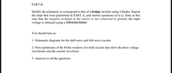
PART B: Modify the schematic to correspond to that of a bridge rectifier using 4 diodes. Repeat the steps that were preformed in PART A, and answer
questions a) to c). Note in this case that the negative terminal of the source is not connected to ground; the input voltage is obtained using a Differential Marker. You should turn in: 1- Schematic diagrams for the half-wave and full-wave circuits. 2- Plots (printouts) of the Probe windows for both circuits that show the three voltage waveforms and the current waveform. 3- Answers to all the
questions.