Page 1 of 1
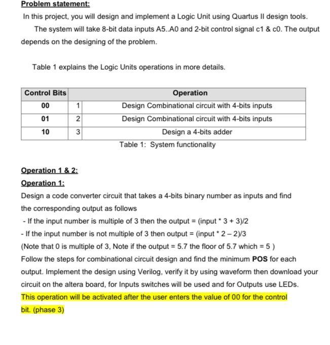
Problem statement: In this project, you will design and implement a Logic Unit using Quartus II design tools. The system
Posted: Fri Jul 01, 2022 5:45 am
by answerhappygod
- Problem Statement In This Project You Will Design And Implement A Logic Unit Using Quartus Ii Design Tools The System 1 (60.81 KiB) Viewed 61 times

- Problem Statement In This Project You Will Design And Implement A Logic Unit Using Quartus Ii Design Tools The System 2 (5.16 KiB) Viewed 61 times
Problem
statement: In this project, you will design and implement a Logic Unit using Quartus II design tools. The system will take 8-bit data inputs A5..A0 and 2-bit control signal c1 & co. The output depends on the designing of the problem. Table 1 explains the Logic Units operations in more details. Control Bits 00 01 10 1 2 3 Operation Design Combinational circuit with 4-bits inputs Design Combinational circuit with 4-bits inputs Design a 4-bits adder Table 1: System functionality Operation 1 & 2: Operation 1: Design a code converter circuit that takes a 4-bits binary number as inputs and find the corresponding output as follows - If the input number is multiple of 3 then the output = (input * 3+3)/2 -If the input number is not multiple of 3 then output = (input *2-2)/3 (Note that 0 is multiple of 3, Note if the output = 5.7 the floor of 5.7 which = 5 ) Follow the steps for combinational circuit design and find the minimum POS for each output. Implement the design using Verilog, verify it by using waveform then download your circuit on the altera board, for Inputs switches will be used and for Outputs use LEDs. This operation will be activated after the user enters the value of 00 for the control bit. (phase 3)
Truth table Simplest SOP in canonical form Design (Minimum cost) to implement.