Page 1 of 1
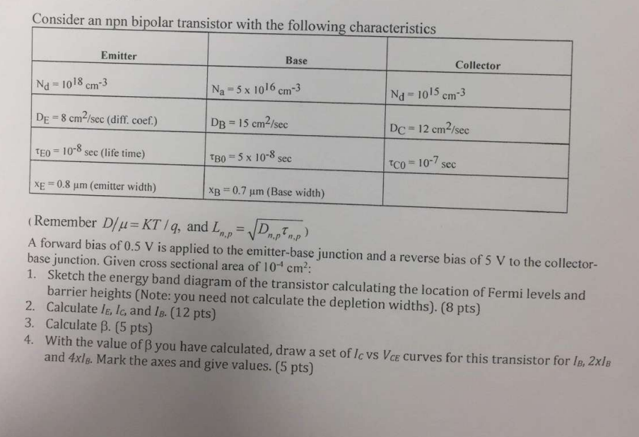
Consider an npn bipolar transistor with the following characteristics Emitter Base Nd=1018 cm-3 Na = 5 x 1016 cm-3 Nd=10
Posted: Tue Jun 07, 2022 12:01 pm
by answerhappygod
- Consider An Npn Bipolar Transistor With The Following Characteristics Emitter Base Nd 1018 Cm 3 Na 5 X 10¹⁶ Cm 3 Nd 10 1 (354.08 KiB) Viewed 61 times
Consider an npn bipolar transistor with the following characteristics Emitter Base Nd=1018 cm-3 Na = 5 x 1016 cm-3 Nd=1015 cm-3 DE = 8 cm²/sec (diff. coef.) DB = 15 cm²/sec Dc = 12 cm²/sec TEO 10-8 sec (life time) TB0= 5 x 10⁻⁸ sec TCO = 10-7 sec XE = 0.8 µm (emitter width) XB = 0.7 µm (Base width) (Remember D/μ = KT / q, and L.p=√ Dn.pn.p) A forward bias of 0.5 V is applied to the emitter-base junction and a reverse bias of 5 V to the collector- base junction. Given cross sectional area of 10 cm²: 1. Sketch the energy band diagram of the transistor calculating the location of Fermi levels and barrier heights (Note: you need not calculate the depletion widths). (8 pts) 2. Calculate IE, IC, and IB. (12 pts) 3. Calculate B. (5 pts) 4. With the value of ß you have calculated, draw a set of Ic vs VCE curves for this transistor for IB,2x1B and 4x1B. Mark the axes and give values. (5 pts) Collector