Page 1 of 1
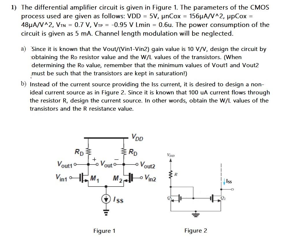
1) The differential amplifier circuit is given in Figure 1. The parameters of the CMOS process used are given as follows
Posted: Thu Jun 02, 2022 9:37 am
by answerhappygod
- 1 The Differential Amplifier Circuit Is Given In Figure 1 The Parameters Of The Cmos Process Used Are Given As Follows 1 (106.01 KiB) Viewed 37 times
1) The differential amplifier circuit is given in Figure 1. The parameters of the CMOS process used are given as follows: VDD = 5V, µnCox = 156μA/V^2, μpCox = 48μA/V^2, VTN = 0.7 V, VTP = -0.95 V Lmin = 0.6u. The power consumption of the circuit is given as 5 mA. Channel length modulation will be neglected. a) Since it is known that the Vout/(Vin1-Vin2) gain value is 10 V/V, design the circuit by obtaining the RD resistor value and the W/L values of the transistors. (When determining the RD value, remember that the minimum values of Vout1 and Vout2 must be such that the transistors are kept in saturation!) b) Instead of the current source providing the Iss current, it is desired to design a non- ideal current source as in Figure 2. Since it is known that 100 uA current flows through the resistor R, design the current source. In other words, obtain the W/L values of the transistors and the R resistance value. VDD RD VDD A Iss + HEM₁ Vout1 o Vin1 0 Vout ERD M₂+ Iss Figure 1 Vout2 -O Vin2 R Figure 2