- Analog Vlsi Laboratory Laboratory 9 Analysis And Design Of Two Stage Operational Amplifier With Miller Compensation Ob 1 (81.39 KiB) Viewed 70 times
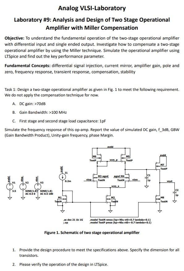
Analog VLSI-Laboratory Laboratory #9: Analysis and Design of Two Stage Operational Amplifier with Miller Compensation Objective: To understand the fundamental operation of the two-stage operational amplifier with differential input and single ended output. Investigate how to compensate a two-stage operational amplifier by using the Miller technique. Simulate the operational amplifier using LTSpice and find out the key performance parameter. Fundamental Concepts: differential signal injection, current mirror, amplifier gain, pole and zero, frequency response, transient response, compensation, stability Task 1: Design a two-stage operational amplifier as given in Fig. 1 to meet the following requirement. We do not apply the compensation technique for now. A. DC gain: >70dB B. Gain Bandwidth: >100 MHZ C. First stage and second stage load capacitance: 1pF Simulate the frequency response of this op-amp. Report the value of simulated DC gain, f_3dB, GBW (Gain Bandwidth Product), Unity-gain frequency, phase Margin. avdd avdd M6 TestP MS TestP vamp e- M7 Testp C1 ppie vinp M3 and Test and M4 Test vinn 0.2m 1p vi vout V2 V3 Vem s 3.5 C2 SINE(1.8T SINE(1.8) AC 0.50 AC 0.5 180 M1 Test M2 Test M8 TestN .ac dec 21 lk 16 j.op model Test nmos (kp=90u vtO=0.7 lambda=0.1) model TestP pmos (kp=40u vto=-0.7 lambda=0.1) Figure 1. Schematic of two stage operational amplifier 1. Provide the design procedure to meet the specifications above. Specify the dimension for all transistors. 2. Please verify the operation of the design in LTSpice.
Task 2: Apply the Miller compensation technique to achieve phase margin greater than 45 degree. Report the value of simulated DC gain, f_3dB, GBW (Gain Bandwidth Product), Unity-gain frequency, phase Margin. Task 3: Apply the Miller compensation along with the lead compensation to achieve phase margin greater than 50 degree. Please try your best to improve the GBW compared to Task 2. Report the value of simulated DC gain, f_3dB, GBW (Gain Bandwidth Product), Unity-gain frequency, phase Margin.