Page 1 of 1
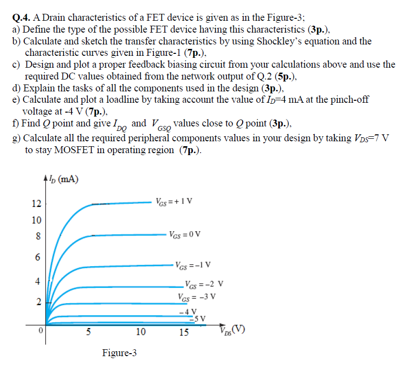
Q.4. A Drain characteristics of a FET device is given as in the Figure-3; a) Define the type of the possible FET device
Posted: Fri May 20, 2022 7:10 pm
by answerhappygod
- Q 4 A Drain Characteristics Of A Fet Device Is Given As In The Figure 3 A Define The Type Of The Possible Fet Device 1 (89.67 KiB) Viewed 50 times
Q.4. A Drain characteristics of a FET device is given as in the Figure-3; a) Define the type of the possible FET device having this characteristics (3p.), b) Calculate and sketch the transfer characteristics by using Shockley's equation and the characteristic curves given in Figure-1 (7p.), c) Design and plot a proper feedback biasing circuit from your calculations above and use the required DC values obtained from the network output of Q.2 (5p.), d) Explain the tasks of all the components used in the design (3p.), e) Calculate and plot a loadline by taking account the value of Id=4 mA at the pinch-off voltage at -4 V (7p.), f) Find Q point and give Ipe and Vo values close to Q point (3p.), DO GSQ g) Calculate all the required peripheral components values in your design by taking Vos=7 V to stay MOSFET in operating region (7p.). AL (mA) 12 VGS =+1 V 10 8 Vas=0 V 6 VGS =-1 V 4 2. Vos=-2 V VGS = -3V - 4 V -5V 15 0 5 10 Vos (V) Figure-3