Page 1 of 1
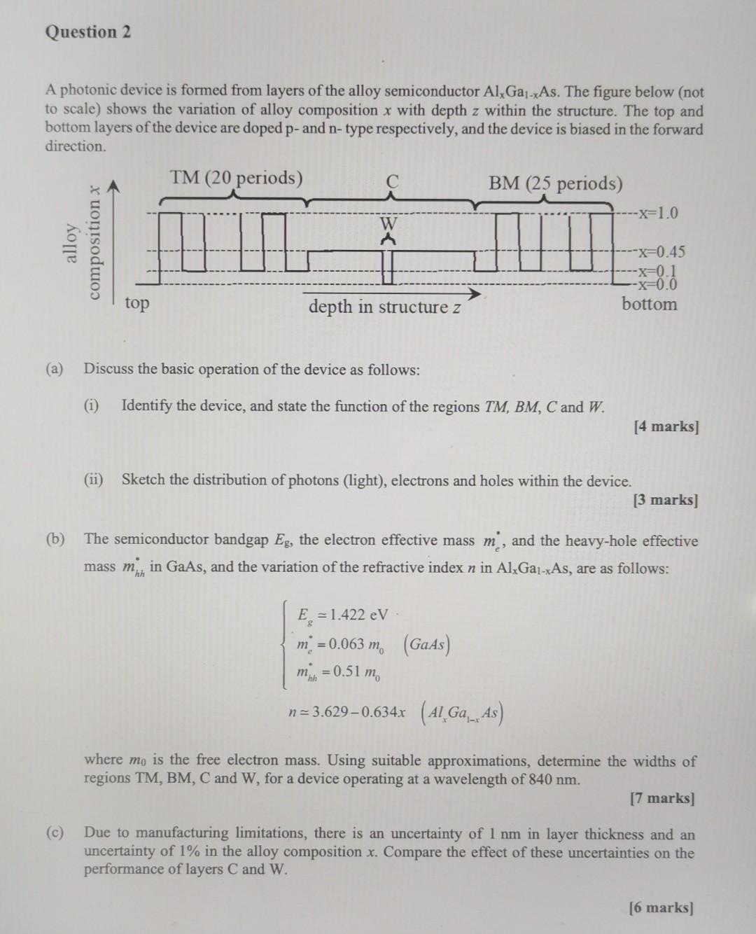
Question 2 A photonic device is formed from layers of the alloy semiconductor Al Ga-xAs. The figure below (not to scale)
Posted: Wed May 18, 2022 4:55 pm
by answerhappygod
- Question 2 A Photonic Device Is Formed From Layers Of The Alloy Semiconductor Al Ga Xas The Figure Below Not To Scale 1 (115.53 KiB) Viewed 64 times
Question 2 A photonic device is formed from layers of the alloy semiconductor Al Ga-xAs. The figure below (not to scale) shows the variation of alloy composition x with depth z within the structure. The top and bottom layers of the device are doped p-and n-type respectively, and the device is biased in the forward p- direction TM (20 periods) BM (25 periods) ---X=1.0 W -X=0.45 -X=0.1 -X=0.0 bottom top depth in structure z (a) Discuss the basic operation of the device as follows: (i) Identify the device, and state the function of the regions TM, BM, C and W. [4 marks] (ii) Sketch the distribution of photons (light), electrons and holes within the device. [3 marks] (b) The semiconductor bandgap Eg, the electron effective mass m, and the heavy-hole effective mass m, in GaAs, and the variation of the refractive index n in Al Gai-xAs, are as follows: hah E -1.422 eV m = 0.063 m(GaAs) min=0.51 m n = 3.629 – 0.634x (Al Ga._, As) where mo is the free electron mass. Using suitable approximations, determine the widths of regions TM, BM, C and W, for a device operating at a wavelength of 840 nm. [7 marks] (c) Due to manufacturing limitations, there is an uncertainty of 1 nm in layer thickness and an uncertainty of 1% in the alloy composition x. Compare the effect of these uncertainties on the performance of layers C and W. [6 marks)