Page 1 of 1
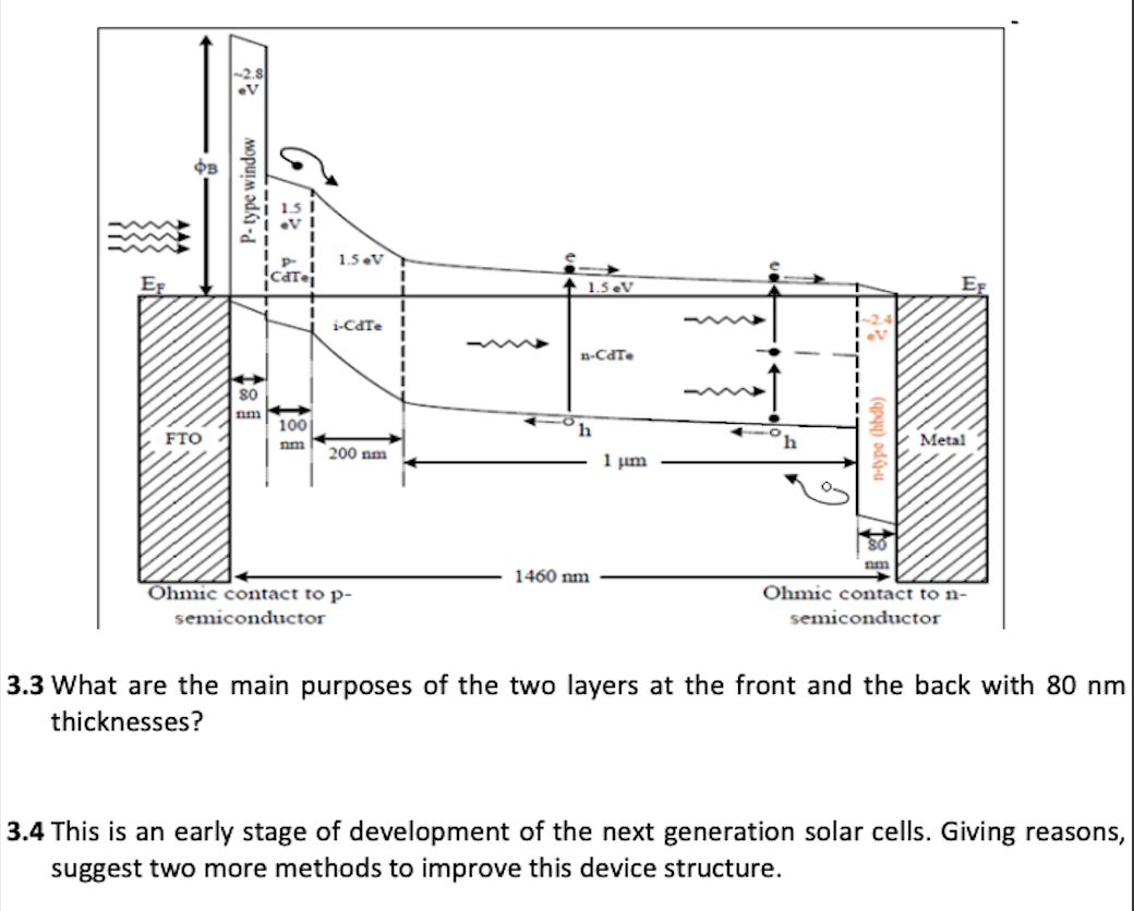
OB P-type window GA 1.5 V 1.5 V EF i-CdTe n-CAT. 80 nm 100 h FTO נות Metal 200 nm 1 m 30 nm 1460 nm Ohmic contact to p-
Posted: Mon May 16, 2022 6:01 am
by answerhappygod
- 1 (236.25 KiB) Viewed 60 times
OB P-type window GA 1.5 V 1.5 V EF i-CdTe n-CAT. 80 nm 100 h FTO נות Metal 200 nm 1 m 30 nm 1460 nm Ohmic contact to p- semiconductor Ohmic contact to n- semiconductor 3.3 What are the main purposes of the two layers at the front and the back with 80 nm thicknesses? 3.4 This is an early stage of development of the next generation solar cells. Giving reasons, suggest two more methods to improve this device structure.