Page 1 of 1
ORE Laboratory 2 Questions_V3 (3) - (Alt+O) NE 管用 設計 插入 版面配置 參考資料 Tifft 校園 已註常 后把 哈共用 說明 Class%20A%20(LWL)-Data%20Sh 97
Posted: Sun May 15, 2022 11:28 pm
by answerhappygod
- 1 (219.87 KiB) Viewed 46 times
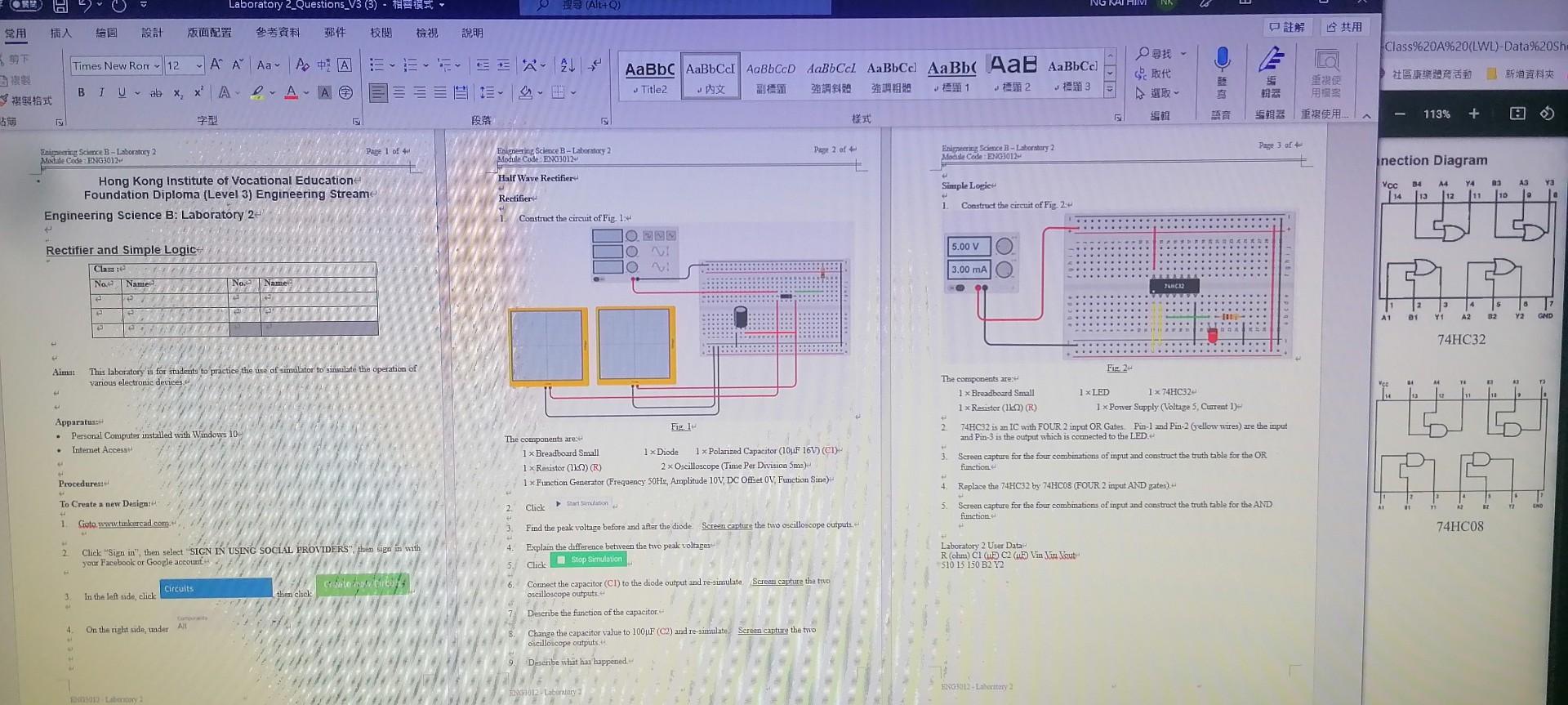
ORE Laboratory 2 Questions_V3 (3) - (Alt+O) NE 管用 設計 插入 版面配置 參考資料 Tifft 校園 已註常 后把 哈共用 說明 Class%20A%20(LWL)-Data%20Sh 97 Times New Rom 12 - A Ă Aa- Pot AEEEEEÄ-21 BIU ab *, * AAA © E Аавьс Аавьсаl | Аавьсср Аавьсаl Аавьсс Аавьс Аав Аавьсс) 內文 強調科 2 尋找。 Exte 建取。 雪碧使 社區產業育活動 「新增資料夾 Title2 山頭1 1993 - 其实指式 占司 樣式 09 字型 段落 音音 组器 113% 重複使用。 + Page 1 of 4 Page 3 of Page 2 of 4 Engneering Science B - Laboratory 2 Medule Code:ENG30124 Engneering Science B-Laboracy 2 Module Code ENG30124 Enigeering Sdce - Laboratory 2 Modele Code 3012 nection Diagram Half Wave Rectifier A3 ya Simple Lopie Vec 34 34 12 Hong Kong Institute of Vocational Educatione Foundation Diploma (Level 3) Engineering Stream- Engineering Science B: Laboratory 24 A4 12 Y4 11 3 10 Rectifier 1 Construct the circuit of Fig. 2- 1 Construct the circuit of Fig. 14 O. 10 N 5.00 V Rectifier and Simple Logic Classe No. Name 3.00 mA No. Name 92 A1 01 Y1 A2 32 Y2 GND 74HC32 Aima: This laboratory is for students to practice the use of simulator to simulate the operation of various electronic devices 13 Apparatus Personal Computer installed with Windows 104 Internet Acces Fie 2- The components are: 1 x Breadboard Small 1 xLED 1 x 74HC32 1x Resistor (I) (R) 1 x Power Supply Voltage 5. Current 1)- 2 74HC32 is an IC with FOUR 2 imput OR Gates. Pin-1 and Pin-2 (rellow wires) are the mput and Pin 3 is the output which is connected to the LED- Sereen capture for the four combinations of input and construct the truth table for the OR function Fig. 1 The components are 1 x Breadboard Small 1 x Diode 1 x Polarized Capacitor (101F 16V) (CT) 1 x Resistor (ILO) (R) 2 x Oscilloscope (Time Per Division 5ms) 1x Function Generator (Frequency 50Hz, Amplitude 10V DC Offset OV. Function Sine) 3 Procedure 4 To Create a new Design Replace the 74HC32 by 74HCOS (FOUR 2 input AND rates)... Screen capture for the four combinations of input and construct the truth table for the AND function 2 Click art. 5 1 Goto
www.linkercad.com 74HC08 Find the peak voltage before and after the diode Screen capture the two oscilloscope outputs.- Explain the difference between the tivo peak voltage Click Stop Simulation 2 Click "Sign in", then select "SIGN IN USING SOCIAL PROVIDERS", then sipa in with your Facebook or Goople account Laboratory 2 User Data R (ohm) CI (C2 (u Vin Sun South 510 15 150 B2 Y2 Circuits crate cure Connect the capacitor (CI) to the diode output and re-simulate Screen capture the tivo oscilloscope outputs 3 In the left side, click then click 4 On the right side under AL Describe the function of the capacitor Change the capacitor valun to 100F (C2) and re-simulate. Screen capture the two oscilloscopir outputs 9. Describe what has happened. 1012 Laboratory ENG02-Laboratory