Page 1 of 1
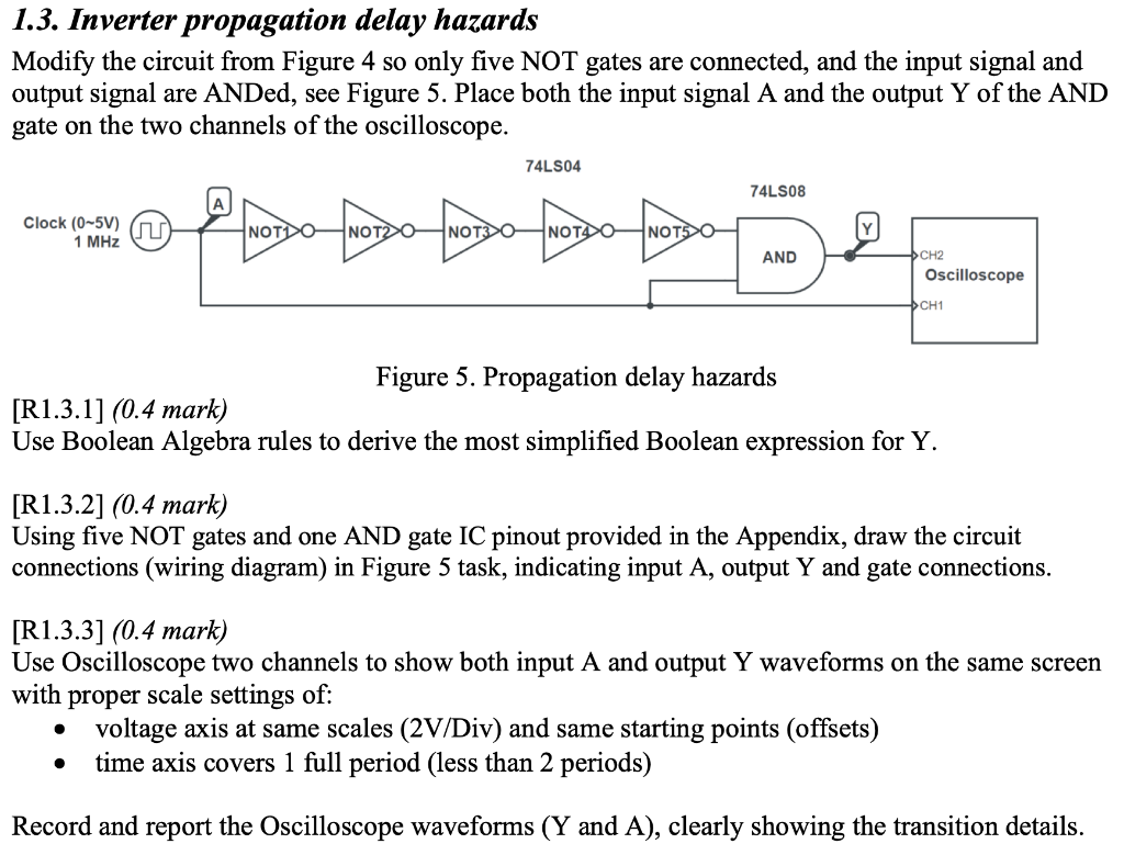
1.3. Inverter propagation delay hazards Modify the circuit from Figure 4 so only five NOT gates are connected, and the i
Posted: Sun May 15, 2022 7:29 pm
by answerhappygod
- 1 3 Inverter Propagation Delay Hazards Modify The Circuit From Figure 4 So Only Five Not Gates Are Connected And The I 1 (191.65 KiB) Viewed 81 times
1.3. Inverter propagation delay hazards Modify the circuit from Figure 4 so only five NOT gates are connected, and the input signal and output signal are ANDеd, see Figure 5. Place both the input signal A and the output Y of the AND gate on the two channels of the oscilloscope. 74LS04 74LS08 Clock (0-5V) 1 MHz NOTDO NOT20 NOTO NOTADO NOTO DE AND CH2 Oscilloscope CH1 Figure 5. Propagation delay hazards [R1.3.1] (0.4 mark) Use Boolean Algebra rules to derive the most simplified Boolean expression for Y. [R1.3.2] (0.4 mark) Using five NOT gates and one AND gate IC pinout provided in the Appendix, draw the circuit connections (wiring diagram) in Figure 5 task, indicating input A, output Y and gate connections. [R1.3.3] (0.4 mark) Use Oscilloscope two channels to show both input A and output Y waveforms on the same screen with proper scale settings of: voltage axis at same scales (2V/Div) and same starting points (offsets) time axis covers 1 full period (less than 2 periods) . . Record and report the Oscilloscope waveforms (Y and A), clearly showing the transition details.