Page 1 of 1
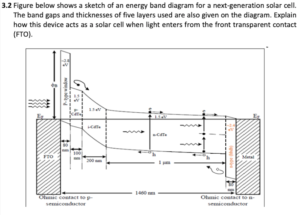
3.2 Figure below shows a sketch of an energy band diagram for a next-generation solar cell. The band gaps and thicknesse
Posted: Sun May 15, 2022 7:20 pm
by answerhappygod
- 3 2 Figure Below Shows A Sketch Of An Energy Band Diagram For A Next Generation Solar Cell The Band Gaps And Thicknesse 1 (237.29 KiB) Viewed 44 times
3.2 Figure below shows a sketch of an energy band diagram for a next-generation solar cell. The band gaps and thicknesses of five layers used are also given on the diagram. Explain how this device acts as a solar cell when light enters from the front transparent contact (FTO). OB P-type window Gr 1.5.V 1.5 eV EF i-Care n.CAT 80 | 11:12 100 nm h FTO Metal 200 nm 1 μm 50 nm 1460 nm Ohmic contact top- semiconductor Ohmic contact to n- semiconductor