Page 1 of 1
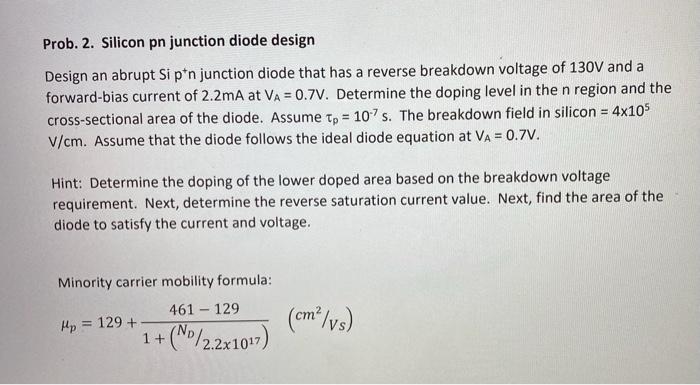
Prob. 2. Silicon pn junction diode design Design an abrupt Sipin junction diode that has a reverse breakdown voltage of
Posted: Sun May 15, 2022 6:03 pm
by answerhappygod
- Prob 2 Silicon Pn Junction Diode Design Design An Abrupt Sipin Junction Diode That Has A Reverse Breakdown Voltage Of 1 (45.48 KiB) Viewed 51 times
Prob. 2. Silicon pn junction diode design Design an abrupt Sipin junction diode that has a reverse breakdown voltage of 130V and a forward-bias current of 2.2mA at VA = 0.7V. Determine the doping level in the n region and the cross-sectional area of the diode. Assume tp = 107s. The breakdown field in silicon = 4x10⁵ V/cm. Assume that the diode follows the ideal diode equation at VA = 0.7V. Hint: Determine the doping of the lower doped area based on the breakdown voltage requirement. Next, determine the reverse saturation current value. Next, find the area of the diode to satisfy the current and voltage. Minority carrier mobility formula: 461 - 129 Mp = 129 + (cm/vs) 1+(N°/2.2x1017)