Page 1 of 1
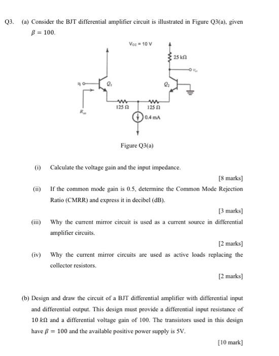
Q3. (a) Consider the BJT differential amplifier circuit is illustrated in Figure Q3(8), given B = 100 Vee = 10 V 25kn w
Posted: Sun May 15, 2022 5:43 pm
by answerhappygod
- Q3 A Consider The Bjt Differential Amplifier Circuit Is Illustrated In Figure Q3 8 Given B 100 Vee 10 V 25kn W 1 (34.38 KiB) Viewed 51 times

- Q3 A Consider The Bjt Differential Amplifier Circuit Is Illustrated In Figure Q3 8 Given B 100 Vee 10 V 25kn W 2 (34.38 KiB) Viewed 51 times
Q3. (a) Consider the BJT differential amplifier circuit is illustrated in Figure Q3(8), given B = 100 Vee = 10 V 25kn w 125 w 125 0.4 m Figure Q3(a) © Calculate the voltage gain and the input impedance. [8 marks] (ii) If the common mode gain is 0.5, determine the Common Mode Rejection Ratio (CMRR) and express it in decibel (dB). [3 marks] (iii) Why the current mirror circuit is used as a current source in differential amplifier circuits. [2 marks] (iv) Why the current mirror circuits are used as active loads replacing the collector resistors. [2 marks] (b) Design and draw the circuit of a BJT differential amplifier with differential input and differential output. This design must provide a differential input resistance of 10 kA and a differential voltage gain of 100. The transistors used in this design have B = 100 and the available positive power supply is 5V. [10 mark]