Page 1 of 1
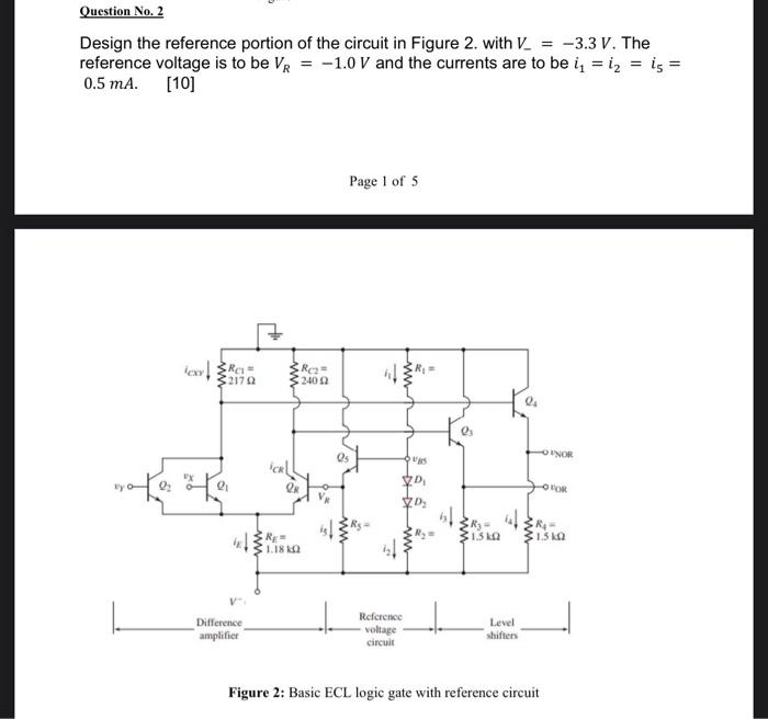
Question No. 2 Design the reference portion of the circuit in Figure 2. with V_ = -3.3 V. The reference voltage is to be
Posted: Sun May 15, 2022 4:02 pm
by answerhappygod
- Question No 2 Design The Reference Portion Of The Circuit In Figure 2 With V 3 3 V The Reference Voltage Is To Be 1 (35.4 KiB) Viewed 56 times
Question No. 2 Design the reference portion of the circuit in Figure 2. with V_ = -3.3 V. The reference voltage is to be VR = -1.0 V and the currents are to be in = iz = is = 0.5 mA. [10] Page 1 of 5 w RO 240 Ω 3217 Os UNOR 0 SOR 2x VD 01 -OHOR D RE ww SIS R 1.5kg Difference amplifier Reference voltage circuit Level shifters Figure 2: Basic ECL logic gate with reference circuit