Page 1 of 1
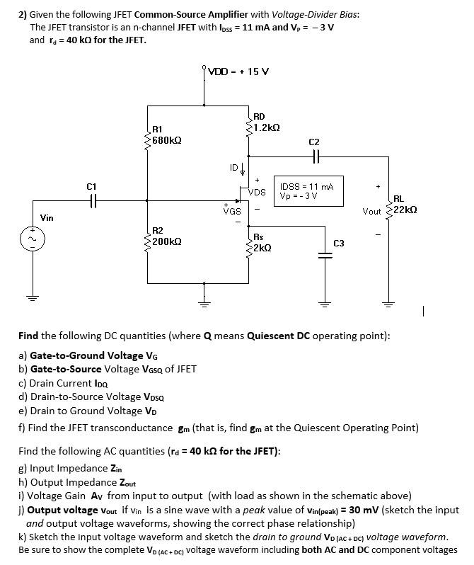
2) Given the following JFET Common-Source Amplifier with Voltage Divider Bias: The JFET transistor is an n-channel JFET
Posted: Sun May 15, 2022 3:54 pm
by answerhappygod
- 2 Given The Following Jfet Common Source Amplifier With Voltage Divider Bias The Jfet Transistor Is An N Channel Jfet 1 (76.19 KiB) Viewed 46 times
2) Given the following JFET Common-Source Amplifier with Voltage Divider Bias: The JFET transistor is an n-channel JFET with loss = 11 mA and VP = -3 V and ra = 40 kn for the JFET. 'YDD = + 15 V RD 1.2kΩ R1 680kΩ C2 HH 10 C1 + VDS IDSS = 11 ma Vp -- 3V HH RL + Vas Vout $220 Vin R2 200kΩ Rs 2kQ C3 Find the following DC quantities (where a means Quiescent DC operating point): a) Gate-to-Ground Voltage VG b) Gate-to-Source Voltage V65Q of JFET c) Drain Current loa d) Drain-to-Source Voltage Vosa e) Drain to Ground Voltage Vp f) Find the JFET transconductance gm (that is, find gm at the Quiescent Operating Point) Find the following AC quantities (rd = 40 ks for the JFET): g) Input Impedance Zin h) Output Impedance Zout i) Voltage Gain Av from input to output (with load as shown in the schematic above) j) Output voltage Vout if Vin is a sine wave with a peak value of Vin(peak) = 30 mV (sketch the input and output voltage waveforms, showing the correct phase relationship) k) Sketch the input voltage waveform and sketch the drain to ground Vo (AC+DC voltage waveform. Be sure to show the complete VO (AC+DC voltage waveform including both AC and DC component voltages )