Page 1 of 1
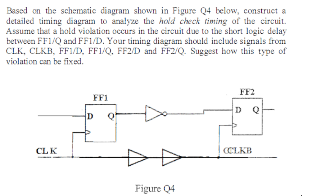
Based on the schematic diagram shown in Figure Q4 below, construct a detailed timing diagram to analyze the hold check t
Posted: Sun May 15, 2022 3:11 pm
by answerhappygod
- Based On The Schematic Diagram Shown In Figure Q4 Below Construct A Detailed Timing Diagram To Analyze The Hold Check T 1 (311.96 KiB) Viewed 38 times
Based on the schematic diagram shown in Figure Q4 below, construct a detailed timing diagram to analyze the hold check timing of the circuit. Assume that a hold violation occurs in the circuit due to the short logic delay between FF1/Q and FF1/D. Your timing diagram should include signals from CLK, CLKB, FF1/D, FF1/Q, FF2/D and FF2/Q. Suggest how this type of violation can be fixed. FF2 FF1 D아 D CLK C'LKB Figure 04