Page 1 of 1
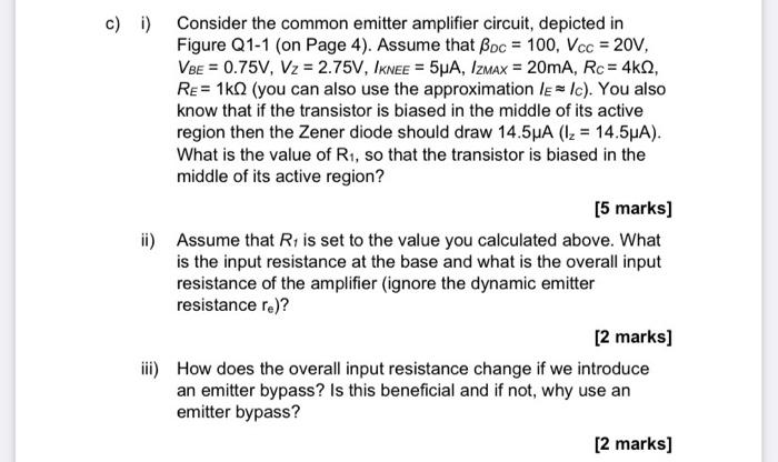
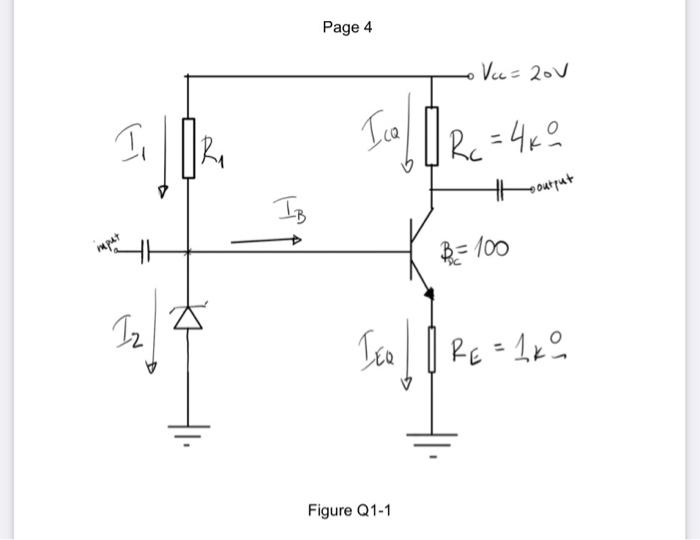
c) i) Consider the common emitter amplifier circuit, depicted in Figure Q1-1 (on Page 4). Assume that Boc = 100, Vcc = 2
Posted: Sun May 15, 2022 2:46 pm
by answerhappygod
- C I Consider The Common Emitter Amplifier Circuit Depicted In Figure Q1 1 On Page 4 Assume That Boc 100 Vcc 2 1 (49.4 KiB) Viewed 48 times
- C I Consider The Common Emitter Amplifier Circuit Depicted In Figure Q1 1 On Page 4 Assume That Boc 100 Vcc 2 2 (19.67 KiB) Viewed 48 times
c) i) Consider the common emitter amplifier circuit, depicted in Figure Q1-1 (on Page 4). Assume that Boc = 100, Vcc = 20V, VBE = 0.75V, V2 = 2.75V, Iknee = 5pA, Izmax = 20mA, Rc = 4k22, RE= 1k02 (you can also use the approximation le = Ic). You also know that if the transistor is biased in the middle of its active region then the Zener diode should draw 14.5uA (Iz = 14.5uA). What is the value of R1, so that the transistor is biased in the middle of its active region? [5 marks] ii) Assume that R is set to the value you calculated above. What is the input resistance at the base and what is the overall input resistance of the amplifier (ignore the dynamic emitter resistance re)? [2 marks] iii) How does the overall input resistance change if we introduce an emitter bypass? Is this beneficial and if not, why use an emitter bypass? [2 marks]
Page 4 Vcc=20v Is 104 피 Ica Rc = 460 th output IB mput BE 100 = Iz Iso | ARC = Leo RE1 Figure Q1-1