Page 1 of 1
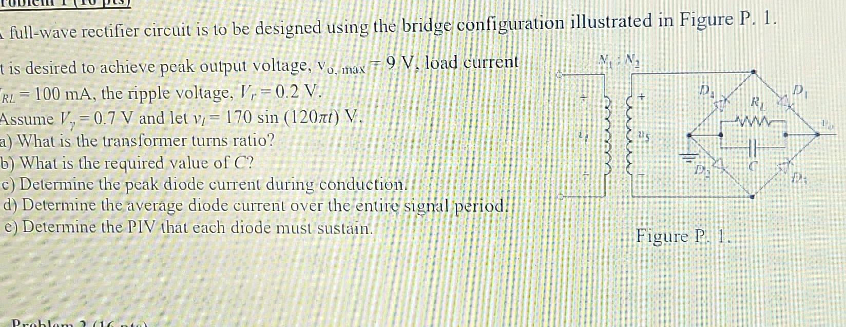
-full-wave rectifier circuit is to be designed using the bridge configuration illustrated in Figure P. 1. :N. D R. w t i
Posted: Mon May 09, 2022 8:15 am
by answerhappygod
- Full Wave Rectifier Circuit Is To Be Designed Using The Bridge Configuration Illustrated In Figure P 1 N D R W T I 1 (281.71 KiB) Viewed 33 times
-full-wave rectifier circuit is to be designed using the bridge configuration illustrated in Figure P. 1. :N. D R. w t is desired to achieve peak output voltage, Vo, max = 9 V, load current RL = 100 mA, the ripple voltage, V, = 0.2 V. Assume 1, = 0.7 V and let v = 170 sin (1207) V. a) What is the transformer turns ratio? b) What is the required value of C? c) Determine the peak diode current during conduction. d) Determine the average diode current over the entire signal period. e) Determine the PIV that each diode must sustain. = D- Figure P.1 Problem to