Page 1 of 1
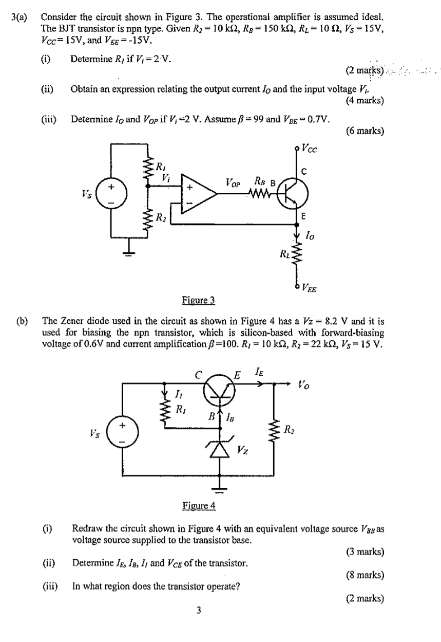
3(a) Consider the circuit shown in Figure 3. The operational amplifier is assumed ideal. The BJT transistor is npn type.
Posted: Mon May 09, 2022 7:58 am
by answerhappygod
- 3 A Consider The Circuit Shown In Figure 3 The Operational Amplifier Is Assumed Ideal The Bjt Transistor Is Npn Type 1 (181.57 KiB) Viewed 31 times
3(a) Consider the circuit shown in Figure 3. The operational amplifier is assumed ideal. The BJT transistor is npn type. Given Ry= 10 kN, Rg = 150 KS2, R2 = 10 N, Vs = 15V, Vcc= 15V, and Vee = -15V. (i) Determine R, if V; = 2 V. (2 marks) . (ii) Obtain an expression relating the output current lo and the input voltage V:. (4 marks) (iii) Determine lo and Vopif V,=2 V. Assume = 99 and VBE = 0.7V. (6 marks) PVCC R с Vi Vop l's WW RB B WWW R E lo RLE VEE Figure 3 (b) The Zener diode used in the circuit as shown in Figure 4 has a Vz = 8.2 V and it is used for biasing the npn transistor, which is silicon-based with forward-biasing voltage of 0.6V and current amplification B=100. R, = 10 k22, R2 = 22 k12, Vs = 15 V. с E TE l'o 11 R Blo + V's R2 V Figure 4 (1) (ii) Redraw the circuit shown in Figure 4 with an equivalent voltage source Vagas voltage source supplied to the transistor base. (3 marks) Determine lɛ, la, I, and Vce of the transistor. (8 marks) In what region does the transistor operate? (2 marks) 3 (iii)