Page 1 of 1
2022 50, Assume Re is fully bypassed. 1. Design a BJT (npn) CE amplifier circuit for the following specifications A. Vol
Posted: Thu May 05, 2022 3:11 pm
by answerhappygod
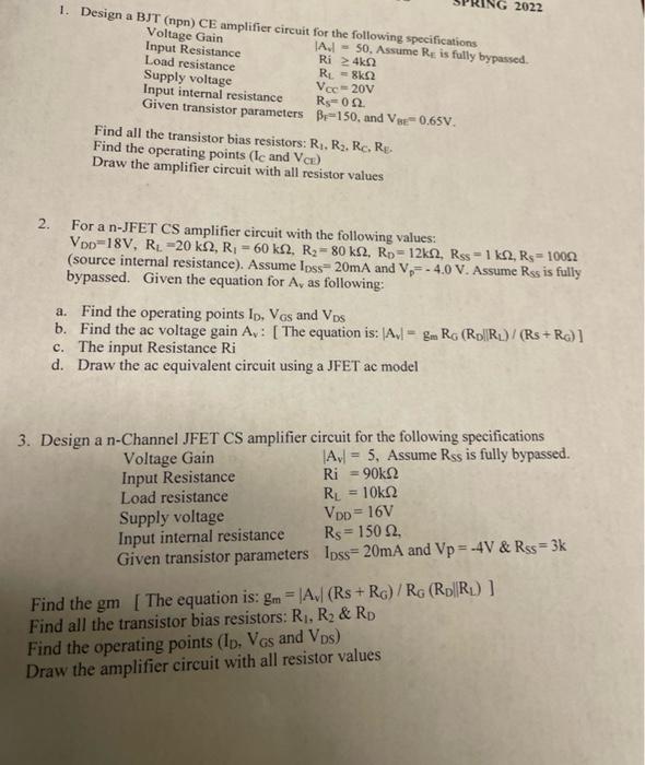
- 2022 50 Assume Re Is Fully Bypassed 1 Design A Bjt Npn Ce Amplifier Circuit For The Following Specifications A Vol 1 (58.49 KiB) Viewed 29 times
2022 50, Assume Re is fully bypassed. 1. Design a BJT (npn) CE amplifier circuit for the following specifications A. Voltage Gain Input Resistance Load resistance Supply voltage Ri 24k R₁ = 8K02 Input internal resistance Vcc=20V Rs 02. Given transistor parameters B-150, and VB 0.65V. Find all the transistor bias resistors: R₁, R₂. Rc. RE. Find the operating points (Ic and VCE) Draw the amplifier circuit with all resistor values 2. For a n-JFET CS amplifier circuit with the following values: VDD 18V, RL -20 k2, R₁ = 60 k2, R₂-80 k2, RD=12k2, Rss=1 k2, Rs 10002 (source internal resistance). Assume Ipss-20mA and V₂-4.0 V. Assume Rss is fully bypassed. Given the equation for A, as following: a. Find the operating points Ip, VGs and VDs B b. Find the ac voltage gain A,: [The equation is: A, gm RG (RDR)/(Rs+ RG)] c. The input Resistance Ri d. Draw the ac equivalent circuit using a JFET ac model 3. Design a n-Channel JFET CS amplifier circuit for the following specifications 5, Assume Rss is fully bypassed. Voltage Gain Av Ri=90k Input Resistance Load resistance Supply voltage R₁ = 10K VDD=16V Rs = 150 2, Input internal resistance Ipss-20mA and Vp = -4V & Rss=3k Given transistor parameters Find the gm [The equation is: gm= |A, (Rs+ RG)/ RG (RD|R₁) ] Find all the transistor bias resistors: R₁, R₂ & RD Find the operating points (ID, VGs and VDs) Draw the amplifier circuit with all resistor values