Page 1 of 1
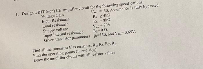
1. Design a BJT (npn) CE amplifier circuit for the following specifications Voltage Gain Av 50, Assume Re is fully bypas
Posted: Thu May 05, 2022 3:04 pm
by answerhappygod
- 1 Design A Bjt Npn Ce Amplifier Circuit For The Following Specifications Voltage Gain Av 50 Assume Re Is Fully Bypas 1 (25.63 KiB) Viewed 33 times
1. Design a BJT (npn) CE amplifier circuit for the following specifications Voltage Gain Av 50, Assume Re is fully bypassed. A Input Resistance Ri 24k R₁ = 8k2 Load resistance Supply voltage Vcc=20V Input internal resistance Rs 0 52. Given transistor parameters B-150, and VBE=0.65V. Find all the transistor bias resistors: R₁, R₂, RC, RE. Find the operating points (le and Ver.) Draw the amplifier circuit with all resistor values