Page 1 of 1
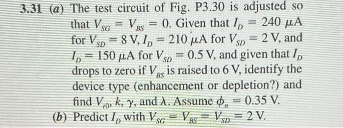
SG D SD SD 3.31 (a) The test circuit of Fig. P3.30 is adjusted so that V so = VBS = 0. Given that I= 240 pA μΑ for Viso
Posted: Mon May 02, 2022 2:46 pm
by answerhappygod
- 1 (40.53 KiB) Viewed 28 times

- 2 (23.38 KiB) Viewed 28 times
- 3 (23.38 KiB) Viewed 28 times
SG D SD SD 3.31 (a) The test circuit of Fig. P3.30 is adjusted so that V so = VBS = 0. Given that I= 240 pA μΑ for Viso = 8 V, 1, = 210 mA for Vso = 2 V, and uA 1, = 150 uA for V sv = 0.5 V, and given that I drops to zero if Ves is raised to 6 V, identify the device type (enhancement or depletion?) and find V70, k, y, and 1. Assume on 0.35 V. (b) Predict 1, with V Vos = Vs = 2V. BS SG BS
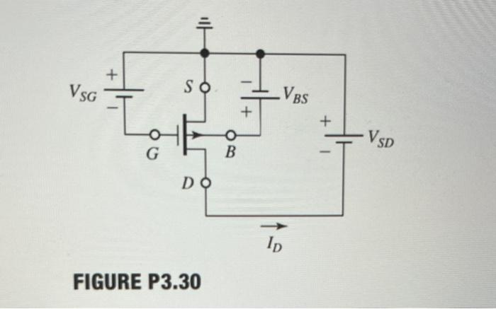
TH + VSG SO VBS + + VSD O B G DO lp FIGURE P3.30