Page 1 of 1
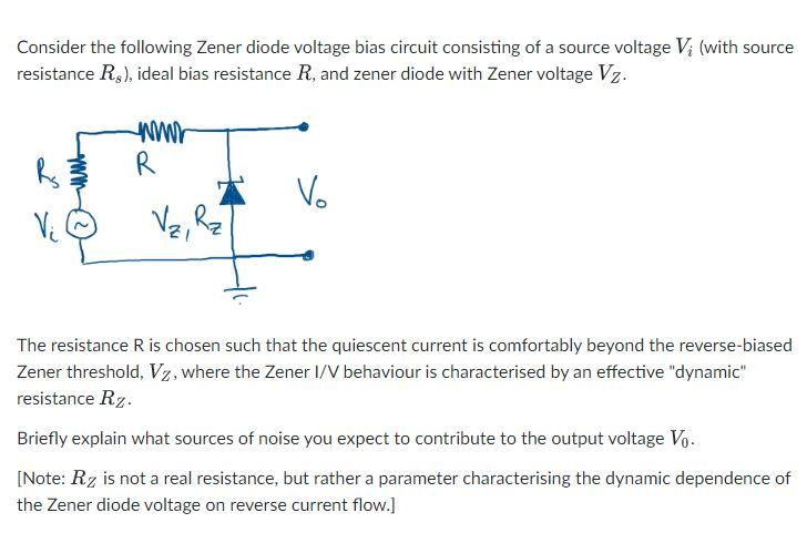
Consider the following Zener diode voltage bias circuit consisting of a source voltage Vi (with source resistance Rs), i
Posted: Mon May 02, 2022 2:23 pm
by answerhappygod
- Consider The Following Zener Diode Voltage Bias Circuit Consisting Of A Source Voltage Vi With Source Resistance Rs I 1 (43.63 KiB) Viewed 27 times
Consider the following Zener diode voltage bias circuit consisting of a source voltage Vi (with source resistance Rs), ideal bias resistance R, and zener diode with Zener voltage Vz. www R w VO Vi V₂, R₂ The resistance Ris chosen such that the quiescent current is comfortably beyond the reverse-biased Zener threshold, V2, where the Zener 1/V behaviour is characterised by an effective "dynamic" resistance Rz. Briefly explain what sources of noise you expect to contribute to the output voltage V. [Note: R2 is not a real resistance, but rather a parameter characterising the dynamic dependence of the Zener diode voltage on reverse current flow.]