Page 1 of 1
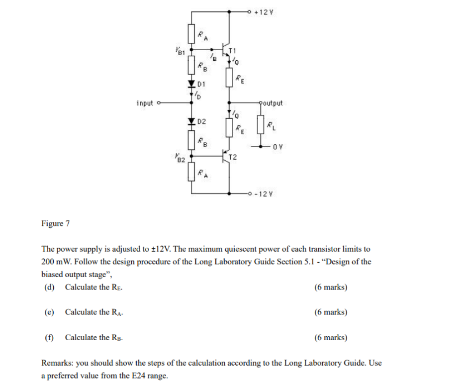
+12 Y le 11 RE 101 140 input goutput 10 D2 [] RE OY 982 1 1 T2 e -0-12 Y Figure 7 The power supply is adjusted to +12V.
Posted: Mon May 02, 2022 1:14 pm
by answerhappygod
- 12 Y Le 11 Re 101 140 Input Goutput 10 D2 Re Oy 982 1 1 T2 E 0 12 Y Figure 7 The Power Supply Is Adjusted To 12v 1 (121.65 KiB) Viewed 47 times
+12 Y le 11 RE 101 140 input goutput 10 D2 [] RE OY 982 1 1 T2 e -0-12 Y Figure 7 The power supply is adjusted to +12V. The maximum quiescent power of each transistor limits to 200 mW. Follow the design procedure of the Long Laboratory Guide Section 5.1 - "Design of the biased output stage”, (d) Calculate the RE. (6 marks) (e) Calculate the RA (6 marks) (1) Calculate the Re. (6 marks) Remarks: you should show the steps of the calculation according to the Long Laboratory Guide. Use a preferred value from the E24 range.